Start With Silicon
All semiconductors rely on silicon to function properly. One of the most common elements on Earth, crude silicon appears in almost any variety of sand. However, suppliers must refine this silicon to nearly 100% purity if it is to function well in electronic applications.
Once it’s pure, workers heat the silicon to a molten state. This allows silicon to develop uniform chemical properties that make it ideal for later applications. After melting and reforming, workers lower a perfectly structured silicon “seed” into a larger vat of molten silicon. This seed creates the ideal conditions for long ingots of high-quality silicon to form.
Silicon’s ability to form long ingots of uniform material enable it to have the strong conductive capabilities that electronic applications rely on. What’s more, silicon is unique in that operators can modify when it can conduct electricity and when it can’t, hence the term “semiconductor.” This on/off capability forms the basis of binary code, i.e. the ones and zeros that dictate computer logic.
Using Photolithography to Pattern Silicon Chips
Manufacturers use photolithography to design the chips for their intended purpose. In this process, workers apply a pattern of photoresist across a wafer to create a “mask,” much like emulsion on film.
After this, workers etch away certain areas of the pattern. They do so by using plasma that degrades material with different properties than the hardened photoresist. Workers and automated processes repeat these steps, as well as deposition, diffusion, and ion implementation processes (outlined below), until they’ve created layers of transistors to their specifications.
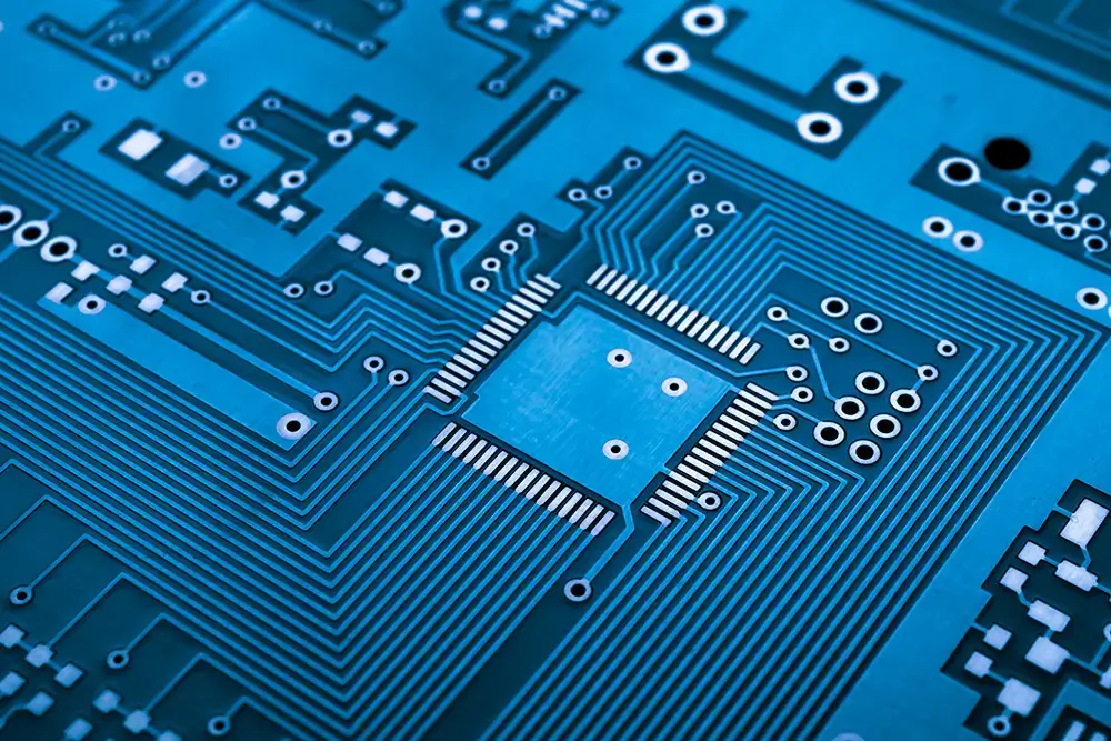
Semiconductor manufacturers then use metallization to form interconnections between different transistors on the chip. This process also forms the chip’s bonding pads, which connect it to the package and the system’s circuit board.
Modifying the Semiconductor For Its Intended Use
Manufacturers perform a number of auxiliary tasks during photolithography to modify the semiconductor for its intended use. The most common processes include:
- Deposition: This process adds an insulating layer to the silicon substrate
- Diffusion: This process bakes impurities into wafer sections to alter their electrical characteristics
- Ion implantation: This process infuses silicon with various dopants to change its electrical characteristics